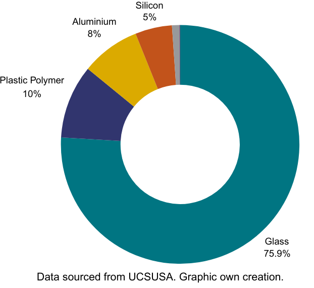
Solar panels are a widely adopted technology for converting sunlight into electricity, often praised as a clean energy solution due to their lack of fossil fuel emissions during use. However, the production process behind solar panels tells a more complex story. While glass makes up the majority of a typical solar panel’s weight (76%), silicon—a critical component—plays a key role in photovoltaic (PV) technology. Approximately 176,640 tons of high-purity silicon are produced annually, serving both the semiconductor and solar panel industries. Crystalline-silicon (c-Si) panels dominate the U.S. market, accounting for 84% of installations, according to the U.S. Department of Energy. Yet, the lifecycle of silicon-based PV panels raises significant environmental concerns.
Silicon, the foundation of PV technology, is the second most abundant element in the Earth’s crust and is commonly found in minerals like quartzite and sandstone ore. To produce the silicon used in solar panels, mining companies extract and refine the material to remove impurities, creating pure silicon or polysilicon. While solar energy remains the largest available energy source on Earth, the environmental impact of current manufacturing processes highlights the need for more sustainable practices.
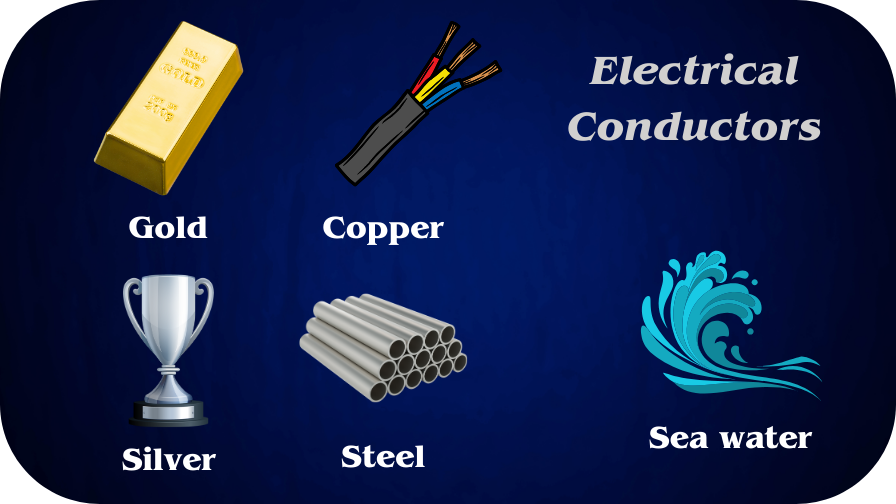
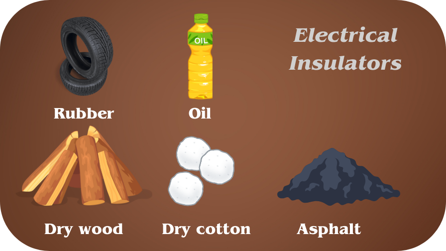
Silicon has unique properties that, after processing and purification, make it a semiconductor material. This means it can conduct electrical energy. Semiconductors can carry electrical currents more effectively than insulators, which do not allow the free flow of electrons, but less effectively than pure conductors, which do. For example, rubber or dry wood are insulators, while materials like silver, steel, or even seawater are conductors. Silicon’s conductivity, however, depends on factors such as ambient temperature and its level of purity.
What is Polysilicon and How Is It Produced?
Polysilicon is made of tiny silicon fragments fused together, giving it unique electrical properties like higher efficiency and better performance in converting sunlight into electricity. Its crystalline structure and higher purity ensure minimal energy loss during the conversion process. To produce polysilicon, silicon undergoes a reduction process where it is heated with a carbon material and oxygen is removed, leaving behind purer metallurgical-grade silicon.
There are two commonly used methods to produce polysilicon, one of which is the Siemens Process. This method achieves the extremely high purity levels needed for solar cell and computer chip production, ranging from 99.99% to 99.99999%. To put this into perspective, silicon with just 1 or 2% impurities is already considered impure and unsuitable for solar panel production.
The Siemens Process starts by mixing silicon pieces with hydrogen chloride to create a liquid called trichlorosilane (TCS). This liquid is unique because it boils at a very low temperature, around 31.8 °C. Thanks to its low boiling point, it can be easily purified by heating it in tall columns, where the pure TCS separates from any remaining impurities.
The next step is the most important. Thin, pure silicon threads are heated to extremely high temperatures, about 1,150°C, inside a sealed container called a bell jar reactor. As the liquid TCS flows over these hot threads, it deposits pure silicon onto them. The threads slowly grow thicker and thicker, much like a candle getting bigger as wax builds up, until they form thick rods about 15 to 20 centimeters wide, roughly the size of a dinner plate. These rods are then broken into smaller pieces.
During this process, a byproduct called silicon tetrachloride is also produced. Rather than letting it go to waste, it is mixed with hydrogen and more ground-up silicon to produce additional TCS liquid. This recycling step boosts the efficiency of the process.
The other method used to produce silicon is called the Fluidized Bed Reactor (FBR). Instead of growing silicon on threads, this method creates small granules of silicon. FBR uses far less electricity than the Siemens Process, requiring only about one-tenth of the energy. However, it comes with its own challenges. The process is complex to run, needs reactors with special protective linings to avoid contamination, and often results in silicon dust waste that cannot be used. Additionally, many patents on this technology limit its accessibility to certain manufacturers.
One major advantage of the FBR method is that it can operate continuously. Unlike the Siemens Process, which needs to pause periodically to remove the silicon rods, FBR can keep producing silicon granules without stopping.
Some manufacturers have found it advantageous to mix equal amounts of silicon chunks from the Siemens Process with granules produced by FBR. Combining the two can make the overall production process faster and more efficient.
Note: Professor Glenmo explains the process in just 2 minutes in a very interactive way which I definitely recommend you to watch:
Key Differences Between Monocrystalline and Polycristalline Solar Panels
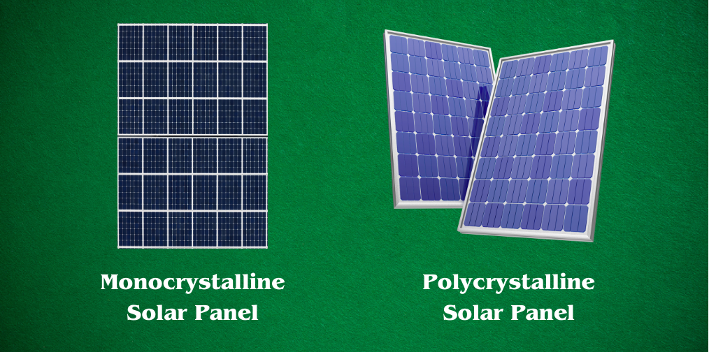
Polycrystalline solar panels typically have lower efficiencies compared to monocrystalline options. This is because each cell contains many crystals, which restrict the movement of electrons. However, their simpler manufacturing process results in a lower price on average. Monocrystalline solar panels, made from a single crystal structure, are more efficient and use purer silicon, which makes them more expensive. In contrast, polycrystalline panels are made from multiple crystal structures, making them more affordable but slightly less efficient.
Polycrystalline panels, made from polysilicon, have a distinctive blue appearance and are more budget-friendly, but they are less efficient at converting sunlight into electricity and perform poorly in hotter conditions. On the other hand, monocrystalline panels, which are black in color, are more expensive but offer higher efficiency, better performance in hot weather, longer lifespan, and a sleeker appearance on rooftops.
High-purity silicon embedded in monocrystalline panels comprise of more complex manufacturing processes, with price ranges lying between $20 to $25 per kilogram. On the other hand, polycrystalline panels are relatively less energy intensive and follow a simpler manufacturing process leading to an average cost of $15 to $20 per kilogram. Given that there are multiple crystalls embedded and meshed together, it can create imperfections leading to lower energy conversion efficiencies. Choosing between the two depends on your budget, energy needs, and aesthetic preferences.
The Polysilicon Market Continues To Grow
The polysilicon market has seen a remarkable recovery following the disruption caused by COVID-19 in 2020. After a sharp decline in production, demand began rebounding in 2021 and is now poised for rapid growth in the coming years. Forecasts made in estimated that by 2024 the market was going to be worth $ 14.49 billion but other sources indicate that by 2023 the market size was already at $ 37.31 billion, with a forecasted compound annual growth rate (CARG) of 16% from 2024 to 2030.1
This expansion of the silicon industry is mostly driven by growth of the solar power industry, with increasing adoption all over the world as a way to generate energy in a cleaner and more sustainable way. In addition, polysilicon production is also closely linked to the growth of the electronics and semiconductor industries. This includes the production of 5G, IoT and AI-driven devices.
In addition, government policies such as taxes, subsidies or tariffs placed on end-products such as solar panels or other silicon-derived products have material impact on its market developments and production generation capacities.
Although the Siemens Process for producing polysilicon originated in Germany, China has refined and adopted the method at scale. This innovation has positioned China as the global leader in polysilicon production, contributing to nearly 80% of the world’s output in 2021.
However, with growing demand and periodic shortages, the industry is likely to diversify geographically in the coming years. Countries in Europe and the United States are expected to play a more significant role in polysilicon production, reducing reliance on a single dominant region.
Environmental, Social and Governance (ESG) Concerns Around Polysilicon Production
The production of polysilicon, a key step after silicon extraction, is highly energy-intensive. Processes such as chemical vapor deposition (CVD) and the Siemens process require extremely high temperatures, reaching approximately 1,150°C. This substantial energy consumption contributes heavily to greenhouse gas emissions, with wafer production alone accounting for about 9% of upstream emissions in semiconductor manufacturing. The process requires careful management of hazardous materials and highly reactive gases to prevent environmental contamination. Although silicon wafers have a lower environmental impact compared to compound semiconductors, the scale of production amplifies these concerns.
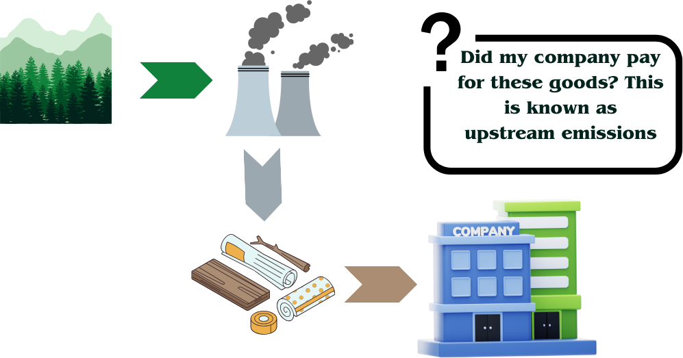
In addition to its energy demands, the manufacturing of silicon wafers generates significant material waste. During the wafer slicing process, 45–55% of the costly silicon is lost in the form of silicon sawdust, also known as kerf. This waste, coupled with the high temperatures (1400–2000°C) required for manufacturing, makes the process both resource-inefficient and environmentally taxing.
To address these challenges, scientists are exploring innovative solutions to recycle silicon sawdust. One promising approach involves transforming this waste into high-performance anode material (e.g. oxidizing metals) for lithium-ion batteries. Through a beads-milling process, researchers have developed nanoflakes with an extremely small thickness (15–17 nm) and a large diameter (0.2–1 μm), offering a cost-effective way to repurpose silicon waste and reduce the environmental impact of wafer production.
When assessing a technology it is not only important to look at the production process, its energy intensity and environmental impact but also it is crucial to perform a social assessment on the supply chain. China is dominant country for silicon extraction and processing into metallurgical-grade silicon (MGS) with around 70% of the market share. According to the US Department of Energy (DOE), 12% of global silicon metal production is used to produce polysilicon for solar panel production. From this 12% of global production, China holds 77% of the global market share. This creates high supply chain dependencies for foreign solar power manufacturers involved in the downstream solar panel production process.
It is important to be aware that most of the Chinese MSG production is concentrated in the Xinjiang region, accounting for 45 percent of global polysilicon production. This region relies heavily on coal-powered plants, exacerbating the environmental impact. Reports have surfaced involving forced labor practices with Uyghurs, a persecuted Muslim ethnic minority, in Xinjiang’s polysilicon plants. There is a lot of controversy and disagreement around this matter still to be clarified to the public. The U.S. has responded with regulations preventing U.S. companies from sourcing materials where products suffer from from forced labor before importing silicon from this region. This includes the US Withhold Release Order and the Uyghur Forced Labor Prevention Act, both of which require companies to verify that their supply chains are free from forced labor before importing silicon from this region.
There’s still a long way to go to make solar panels truly sustainable. This article only scratches the surface, focusing on silicon. While technological innovation is crucial, it’s not the whole solution. Consumers and policymakers need to stay engaged with supply chain developments and production methods to make informed, conscious choices.
There are exciting advancements, like kerfless wafer production, which could significantly reduce material waste, and ongoing research is working to improve energy efficiency in manufacturing. But the real challenge is finding a balance—meeting the growing demand for these vital technologies while minimizing their environmental impact and ensuring ethical production practices. With the semiconductor and solar industries expanding rapidly, developing more sustainable and socially responsible methods isn’t just important; it’s essential.
- Compounded annual growth rate (CARG) divides the final value against the initial value raised to the exponent of 1 divided by the number of periods under study. For example, if my initial value is $100 and my final value is $1,000 over a period of 10 years, this would mean a CARG of 25.89%. You can check more details here and an online calculator here. ↩︎
References & Further Study
Web Articles:
- Let’s Go Solar. (n.d.). How are solar panels made? Retrieved from https://www.letsgosolar.com
- Union of Concerned Scientists. (n.d.). What’s in a solar panel? Retrieved from https://blog.ucsusa.org
- U.S. Department of Energy. (n.d.). Solar photovoltaic manufacturing basics. Retrieved from https://www.energy.gov
- ThoughtCo. (n.d.). Examples of electrical conductors and insulators. Retrieved from https://www.thoughtco.com
Industry Sources:
- Tongwei. (n.d.). Polysilicon and its role in solar energy. Retrieved from https://en.tongwei.com.cn
- RatedPower. (n.d.). Polysilicon definition. Retrieved from https://ratedpower.com
- Grand View Research. (n.d.). Polysilicon market analysis. Retrieved from https://www.grandviewresearch.com
- Mordor Intelligence. (n.d.). Polysilicon market trends and growth. Retrieved from https://www.mordorintelligence.com
Technical Resources:
- ICICI Direct. (n.d.). CAGR calculator. Retrieved from https://www.icicidirect.com
- Persefoni. (n.d.). Upstream vs downstream in supply chains. Retrieved from https://www.persefoni.com
- Hitachi High-Tech. (n.d.). Semiconductor glossary. Retrieved from https://www.hitachi-hightech.com
- WaferPro. (n.d.). What is polysilicon? Retrieved from https://waferpro.com
Scientific and Environmental Analysis:
- Interface. (n.d.). Chip production’s ecological footprint. Retrieved from https://www.interface-eu.org
- Atlas Scientific. (n.d.). Why does conductivity increase with temperature in semiconductors? Retrieved from https://atlas-scientific.com
- EcoFlow. (n.d.). Effects of temperature on solar panel efficiency. Retrieved from https://blog.ecoflow.com
Video Resources:
- Energy Information Administration. (n.d.). Photovoltaics and electricity. Retrieved from https://www.eia.gov
- Geotherm HVAC. (n.d.). Mono vs poly: Which is better? Retrieved from https://www.geothermhvac.com
- YouTube. (n.d.). How are solar panels made? Retrieved from https://www.youtube.com


